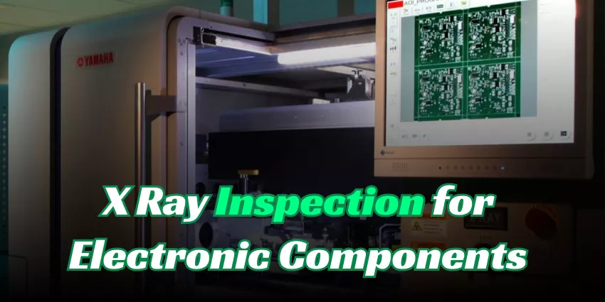
X-ray inspection for electronic components is a non-destructive testing method that employs X-rays to scrutinize internal structures. This crucial technique ensures quality, reliability, and precise analysis without physically altering the components.
In this passage, let's see how X-ray inspection for electronic components works.
What is X-ray inspection for Electronic Components
X-ray inspection for electronic components is a non-destructive testing method used to examine the internal structure and integrity of various electronic devices, assemblies, and components. X-ray inspection provides detailed insights into the quality, reliability, and functionality of electronic components without requiring physical disassembly or damage to the item being inspected.
Here are some key points regarding X-ray inspection for electronic components:
-
Purpose:
- X-ray inspection is commonly used in the electronics industry to detect defects, faults, and anomalies such as solder joint quality, component placement accuracy, wire bond integrity, voids in solder, and foreign object debris (FOD).
-
Components Inspected:
- This method is suitable for inspecting various electronic components, including printed circuit boards (PCBs), integrated circuits (ICs), ball grid arrays (BGAs), packaged chips, connectors, lead frames, and other electronic assemblies.
-
How it Works:
- X-ray inspection involves passing X-ray radiation through the electronic component or assembly. The X-rays are absorbed differently by materials of varying densities, resulting in an image that highlights the internal features and structures of the component in high resolution.
-
Types of X-ray Inspection:
- 2D X-ray imaging: Provides a two-dimensional image of the internal structure of the component.
- 3D X-ray imaging or computed tomography (CT): Offers a three-dimensional view of the internal features, enabling detailed analysis of complex structures and potential defects.
-
Benefits:
- Non-destructive: Allows inspection of components without causing damage, making it suitable for assessing the quality of high-value or sensitive electronic parts.
- Defect Detection: Helps identify defects such as solder bridges, voids, cracks, shorts, and insufficient or excess solder.
- Quality Control: Enables quality assurance by verifying internal connections, component placement, and overall assembly quality.
- Failure Analysis: Facilitates root cause analysis of component failures, enabling corrective actions to be implemented.
-
Applications:
- X-ray inspection is utilized in various industries, including automotive, aerospace, consumer electronics, medical devices, telecommunications, and more, where high reliability and quality standards are essential.
-
Regulatory Compliance:
- X-ray inspection can aid in meeting regulatory requirements and standards for electronic components, especially in safety-critical applications or industries with stringent quality control measures.
Overall, X-ray inspection plays a crucial role in ensuring the reliability, functionality, and quality of electronic components, assemblies, and devices during manufacturing, quality control, and failure analysis processes.
How Does X-Ray Inspection for Electronic components work
X-ray inspection for electronic components is a valuable technique used to examine the internal structure and integrity of electronic assemblies without causing physical damage. Here's how X-ray inspection works for electronic components:
-
X-ray Source:
- X-ray inspection systems include an X-ray source that emits X-ray radiation. The source can be a tube generating X-rays at various energy levels, typically ranging from a few to hundreds of kilovolts.
-
Sample Preparation:
- The electronic component or assembly to be inspected is placed on a sample stage inside the X-ray inspection system. The component should be positioned to allow the X-rays to pass through it.
-
X-ray Exposure:
- The X-ray source emits X-rays that pass through the electronic component. The X-rays interact differently with various materials within the component based on their densities and thicknesses.
-
Detection System:
- A detector placed opposite the X-ray source captures the X-rays that pass through the component. The detector converts the X-ray signals into electrical signals for further processing.
-
Image Formation:
- The transmitted X-rays produce a shadow image on the detector. The areas with higher density or thicker materials in the component absorb more X-rays and appear as darker regions on the X-ray image.
-
Image Processing:
- The captured X-ray image is processed and enhanced by the X-ray inspection system's software. This process helps highlight internal structures, defects, and anomalies within the electronic component or assembly.
-
Analysis and Interpretation:
- The processed X-ray image is analyzed by trained operators or automated algorithms. They interpret the X-ray image to identify defects such as solder joint quality, voids, cracks, misalignments, component placement issues, and other anomalies.
-
3D X-ray Inspection (CT):
- For more complex structures or to analyze internal features in three dimensions, computed tomography (CT) can be employed. CT scans involve taking multiple X-ray images from different angles and reconstructing them into a 3D model using specialized software.
-
Reporting:
- Inspection results and findings are documented in reports, detailing detected defects or areas of concern. This information is crucial for quality control, failure analysis, and process optimization.
X-ray inspection is a powerful tool in the electronics industry, offering non-destructive testing capabilities for assessing the quality, reliability, and functionality of electronic components and assemblies. It enables manufacturers to detect and address issues early in the production process, ensuring the delivery of high-quality and reliable electronic products to customers.
Benefits of X-Ray Inspections for Electronic Components
X-ray inspection for electronic components offers numerous benefits that make it a valuable tool in various industries, particularly in electronics manufacturing and quality control. Some of the key benefits of X-ray inspections for electronic components include:
-
Non-Destructive Testing: X-ray inspection allows for the examination of internal structures of electronic components without causing any physical damage. This non-destructive testing method preserves the integrity of the components, enabling thorough inspection without compromising their functionality.
-
Defect Detection: X-ray inspections can identify a wide range of defects within electronic components, such as solder joint quality, voids, cracks, shorts, misalignments, foreign object debris (FOD), and other manufacturing defects. This helps in ensuring the overall quality and reliability of the components.
-
Component Placement Verification: X-ray inspections can verify the accuracy of component placement on printed circuit boards (PCBs) and other assemblies. It helps in detecting misaligned or missing components, ensuring that the assembly meets design specifications.
-
Internal Structure Visualization: X-ray imaging provides detailed insights into the internal structures of electronic components, allowing for the detection of hidden defects and anomalies that may not be visible through external inspection methods.
-
Quality Control: X-ray inspections play a crucial role in quality control processes by enabling manufacturers to detect and address production issues early in the manufacturing process. This ensures that only high-quality components are delivered to customers.
-
Root Cause Analysis: In the event of component failures or performance issues, X-ray inspections can be used for root cause analysis. By examining internal structures and identifying defects, manufacturers can determine the underlying reasons for failures and implement corrective actions.
-
Process Optimization: X-ray inspections help in optimizing manufacturing processes by identifying areas for improvement, reducing defects, and enhancing overall production efficiency. This leads to higher yields and improved product quality.
-
3D Imaging Capability: With computed tomography (CT) technology, X-ray inspections can provide three-dimensional imaging of electronic components and assemblies. This advanced imaging capability offers detailed visualization of complex structures and facilitates in-depth analysis.
-
Regulatory Compliance: X-ray inspections help manufacturers comply with industry standards, regulations, and certifications by ensuring that electronic components meet safety and quality requirements. It demonstrates a commitment to producing reliable and compliant products.
-
Cost-Effective Solution: While X-ray inspections are a sophisticated technology, they offer a cost-effective solution for identifying defects and ensuring the quality of electronic components. The ability to detect issues early on can prevent costly recalls and rework in the long run.
Overall, X-ray inspections for electronic components provide a valuable means of ensuring product quality, reliability, and performance in the electronics industry. By leveraging this technology, manufacturers can enhance their quality control processes, minimize defects, and deliver high-quality electronic products to the market.
Final Verdict
X-ray inspection is a valuable tool in quality control and assurance processes, especially in industries where precise and non-destructive analysis of internal structures is crucial. After reading this passage, hopefully, you'll have a comprehensive understanding of how X-ray inspection for electronic components works and its benefits.